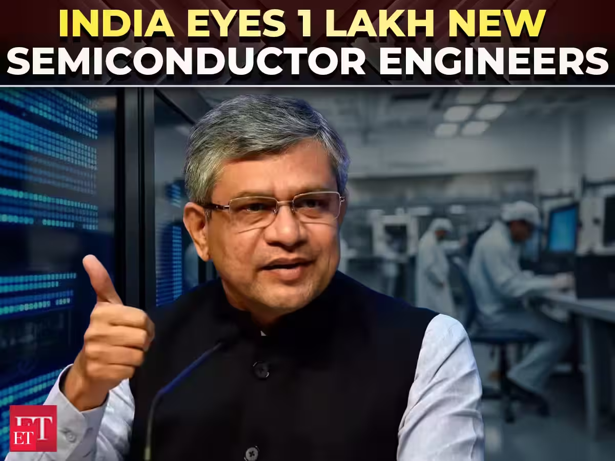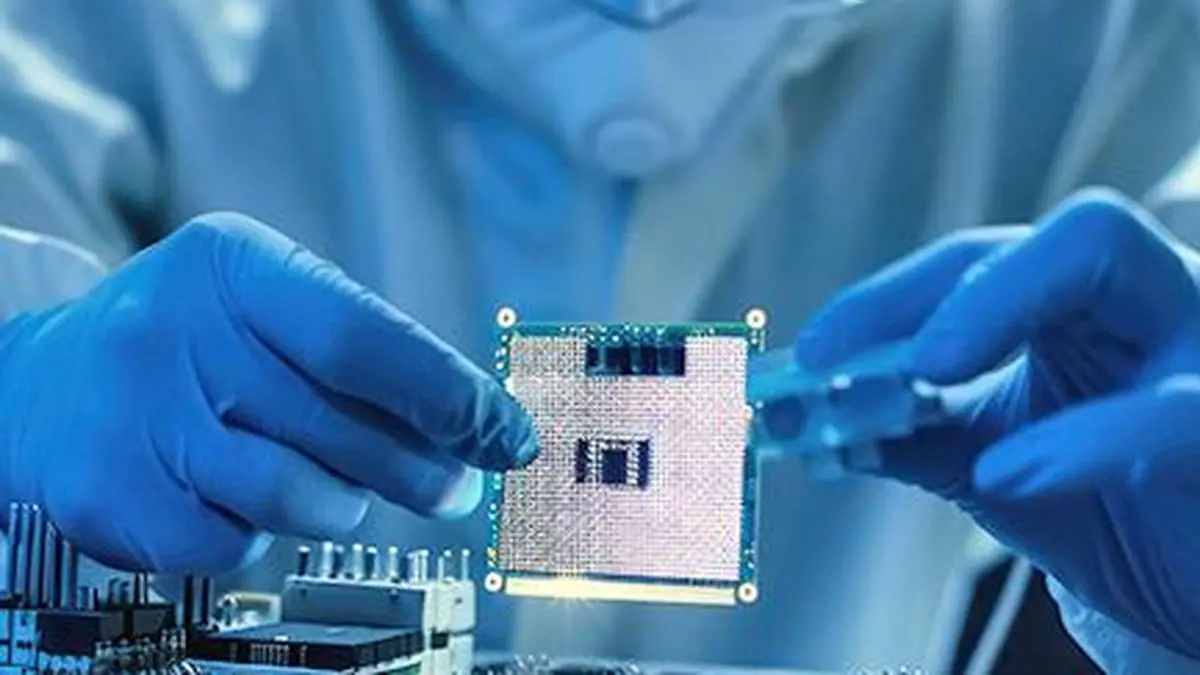
The move comes at a time when semiconductors have emerged as a critical strategic resource globally.
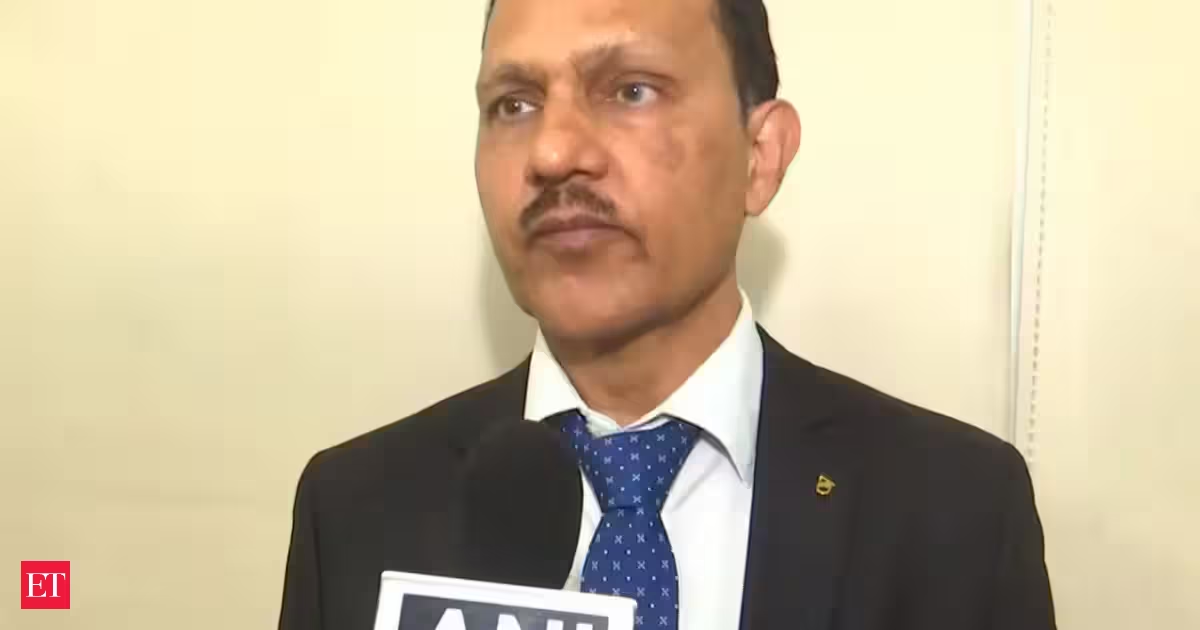
The Centre on Monday notified the Semicon 2.0 scheme, setting in motion the ₹1,27,500-crore plan that seeks to deepen India’s semiconductor ambitions – charting out eligibility and incentives across the semiconductor value chain, including 40 per cent fiscal support on pari-passu basis for silicon wafer fabs with a minimum investment of ₹20,000 crore, and sweeteners for chip design.The scheme was approved by the Union Cabinet on July 15, 2026 and the Gazette notification on Monday spells out the contours of the new programme detailing how the ₹1,27,500-crore outlay will be implemented, and how incentives will be structured, and the eligibility criteria for various categories.The Semicon 2.0 has six pillars including Design of semiconductor IPs, chips, system-on-chips (SoCs), and modules for national importance; machines and materials; setting up more fabs; further strengthening the ATMP/OSAT industry; R&D for advanced semiconductor technologies; and talent development.“India achieved its target of developing 85,000 semiconductor engineers over a period of 10 years in just four years, and has now set a new target of developing one-lakh more engineers. In the coming years, close to 10 per cent of the global semiconductor industry’s market is expected to be in India. Students from tier-II and tier-III cities have already designed more than 250 chips,” Ashwini Vaishnaw, Minister of Electronics and IT, told reporters here.In one case, commercial production commenced within just 13 months of the groundbreaking, while approvals were granted within 200 days, 150 days and even 90 days in multiple cases, he noted.“The semiconductor ecosystem being developed in India is also expected to create 50,000–60,000 direct jobs. Projects supported under Semicon 2.0 will generally have a duration of up to six years, while the scheme will initially remain open for applications for three years,” he added.The move comes at a time when semiconductors have emerged as a critical strategic resource globally, with the artificial intelligence (AI) boom driving unprecedented demand for advanced chips and memory. At the same time, growing concerns over supply-chain vulnerabilities and shifting geopolitics have pushed global players to expand semiconductor capacities and reduce dependence on concentrated production hubs.“The main objective of this scheme is of course to develop self reliant to the globally competitive semiconductor industry; development of the design and manufacturing a complete ecosystem in the country because one important thing which is essential for the semiconductor is all the ecosystem players have to be there,” S Krishnan, Secretary, Ministry of Electronics and Information Technology (MeitY), said.The time was ripe now to move to next stage to develop semiconductor ecosystem through Semicon 2.0. The objective of the scheme is self reliance and fostering a globally competitive industry, Krishnan added.“The speed with which the government has moved from Cabinet approval to official notification sends a strong message of policy continuity, execution and commitment. For an industry that makes investments with a 10–15 year horizon, this continuity provides the confidence required for long-term investments,” Ashok Chandak, President, India Electronics and Semiconductor Association (IESA) and SEMI India, said.Published on August 31, 2026