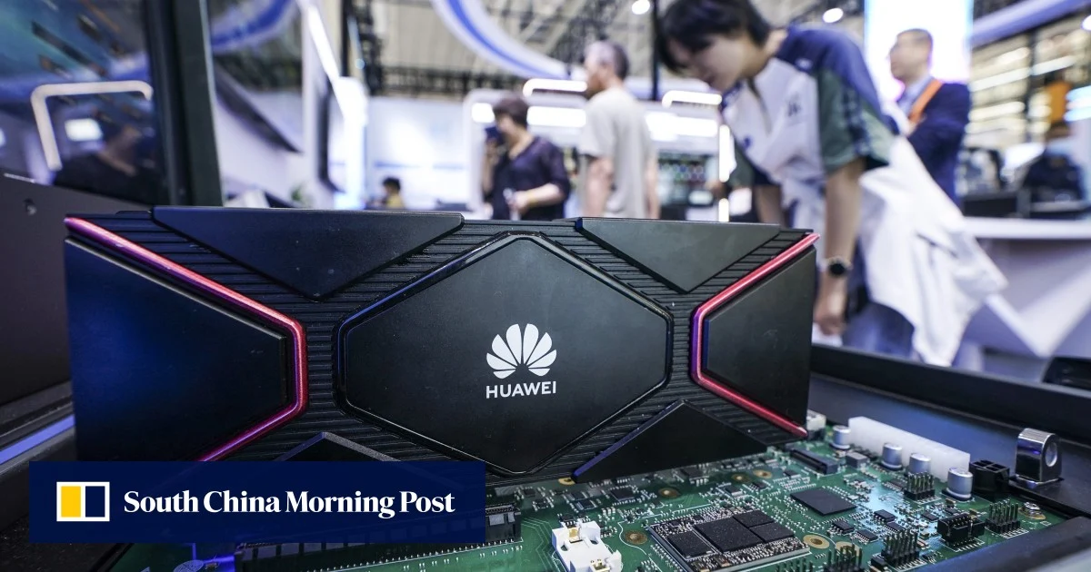
As global chip companies approach physical limits in their pursuit of more powerful processors, Huawei Technologies Co's emphasis on improving transmission speeds between system components could offer an alternative path, experts said.
The comments come as industry watchers recognize a systematic, replicable innovation ecosystem taking shape across China's tech landscape, spanning semiconductor design, memory chip fabrication, artificial intelligence frameworks and system integration.
Liao Heng, chief semiconductor scientist at Huawei, said in a recent four-hour interview that the decades-long practice of continuously shrinking transistors and packing more into integrated circuits is running out of runway, as transistors are now almost as small as atoms, nearing the physical extreme of contemporary manufacturing capabilities.
While Western companies have multiyear road maps enabled by ASML's advanced lithography machines, Huawei — barred from accessing such equipment due to sanctions imposed by the United States government — has had to pursue a more creative approach, Liao said.
That approach is Huawei's "Tau Scaling Law", proposed in May, which shifts focus from shrinking chip dimensions to improving transmission speeds between system components.