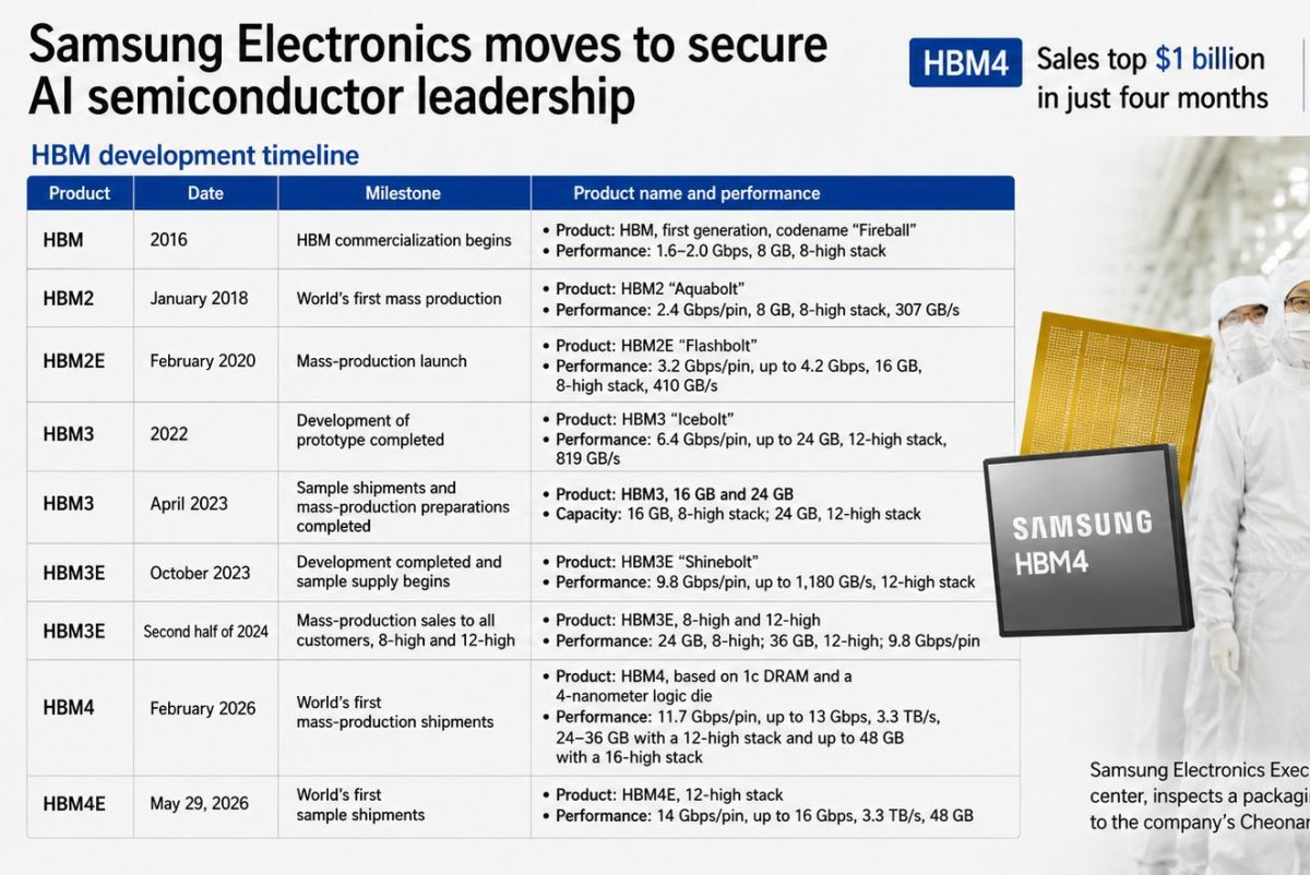
Samsung Electronics Executive Chairman Jay Y. Lee, center, inspects a packaging line during a 2023 visit to the company’s Cheonan campus. Data from Samsung Electronics. Infographic by Asia Today and translated by UPI
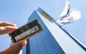
June 23 (Asia Today) -- Samsung Electronics Executive Chairman Jay Y. Lee visited the company's Cheonan campus Tuesday for the first time in more than three years to inspect high-bandwidth memory packaging operations as competition intensifies in the market for artificial intelligence chips.
Lee toured the C1 and C2 production lines at the campus in Cheonan, about 53 miles south of Seoul, Samsung Electronics said.
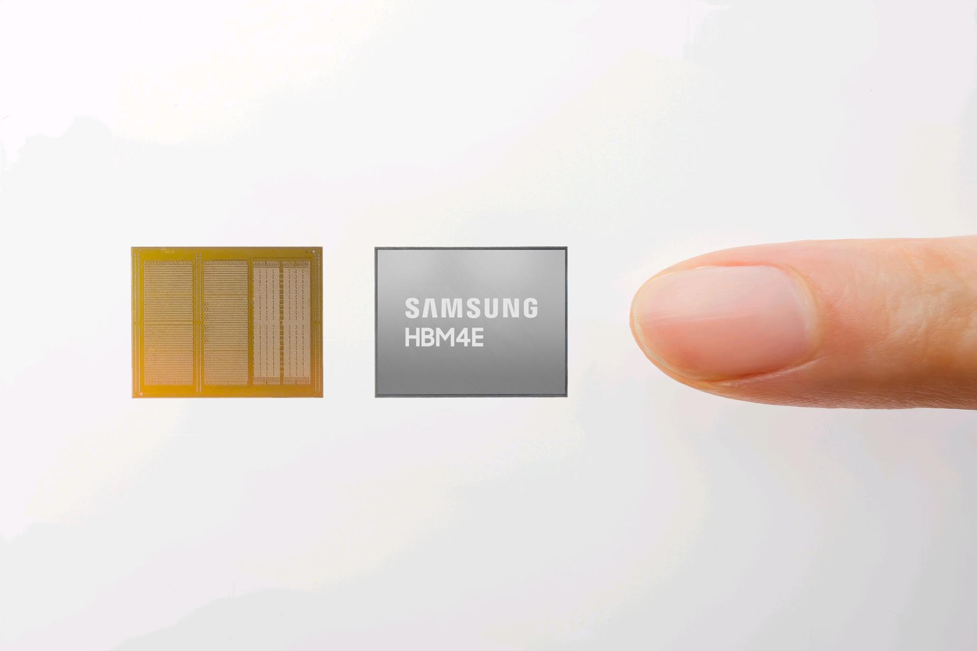
After receiving briefings on plant operations, production plans and technology development, Lee put on a cleanroom suit and inspected an HBM packaging line. He reviewed the operation's production capacity and quality control systems.
The Cheonan campus is a major production center for Samsung's HBM back-end processing and advanced packaging.