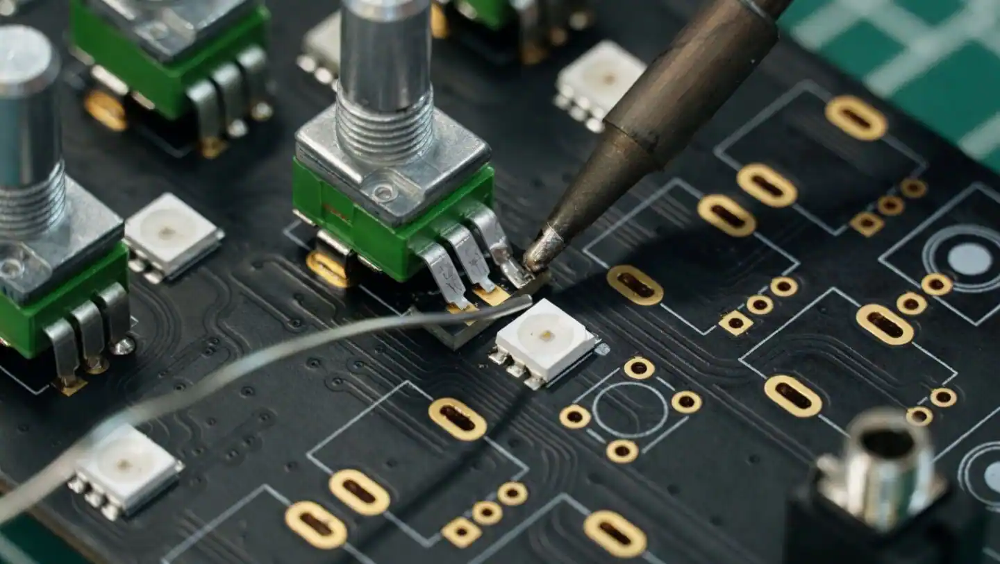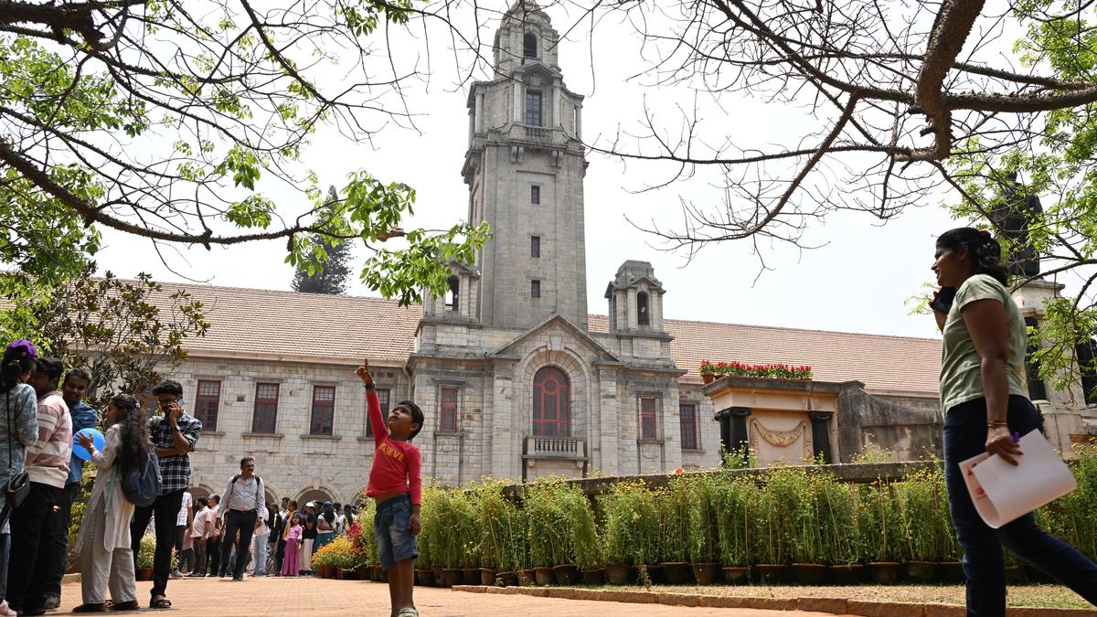
The Semiconductor Training Fabrication (Fab) Facility is located in the Centre for Nano Science and Engineering (CeNSE) in the Indian Institute of Science (IISc), Bengaluru.
| Photo Credit: ALLEN EGENUSE J
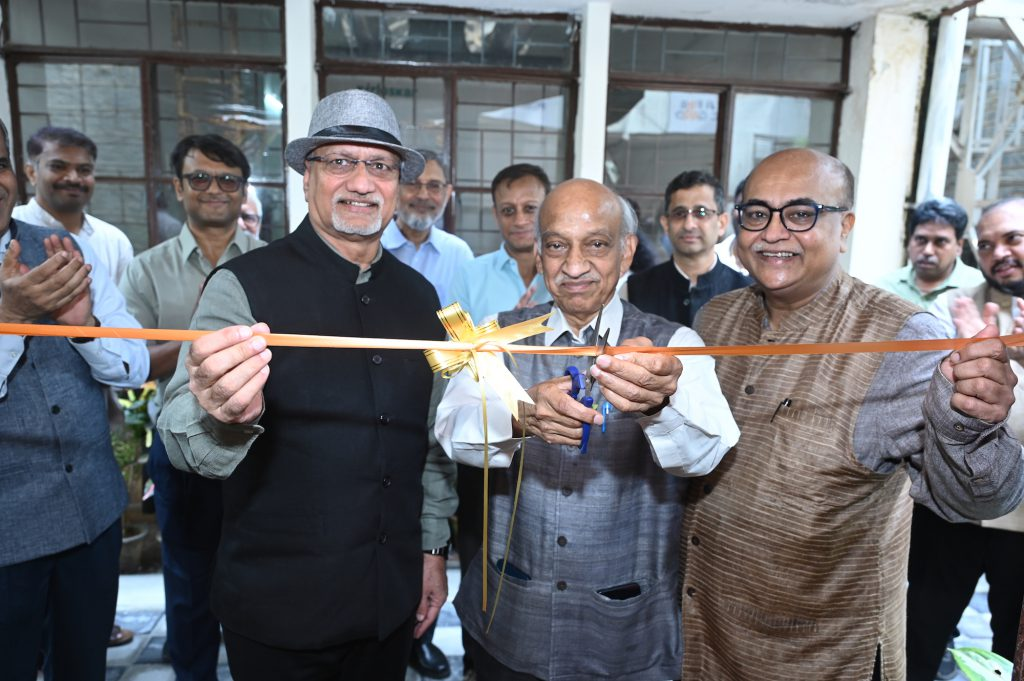
President Droupadi Murmu inaugurated the Semiconductor Training Fabrication (Fab) Facility at the Centre for Nano Science and Engineering (CeNSE) in the Indian Institute of Science (IISc), Bengaluru via video conferencing, on June 3.Established with support from the Ministry of Tribal Affairs (MoTA), the facility is a step towards building a skilled and inclusive semiconductor workforce for the nation.The Semiconductor Training Fab has been created to provide hands-on, industry-relevant training in semiconductor fabrication, microfabrication processes, cleanroom operations, device manufacturing, and characterisation techniques.The facility is expected to play an important role in addressing the growing demand for skilled manpower required by India’s rapidly expanding semiconductor and electronics manufacturing ecosystem.CeNSE said the facility builds upon a successful semiconductor skilling programme launched by IISc CeNSE with support from the Ministry of Tribal Affairs.Since its inception, the programme has trained more than 1,400 participants from Scheduled Tribe communities, delivered over 48,000 hours of specialised semiconductor training, and awarded more than 1,000 NSQF certifications.The initiative has achieved nationwide reach, engaging participants from over 30 States and Union Territories, and more than 273 institutions, including IITs, NITs, universities, and colleges.The newly-inaugurated training fab features a dedicated 3,200 sq. ft. semiconductor cleanroom facility equipped with advanced semiconductor processing and characterisation tools.Designed specifically for training and workforce development, the facility will provide experiential learning opportunities that bridges the gap between academic education and semiconductor manufacturing practice.It is expected to train up to 700 students annually through foundational and advanced semiconductor training programmes, and also outreach through diploma-level industry exposure initiatives, and school outreach programmes.CeNSE said the programme has already demonstrated meaningful impact as several participants have progressed to advanced research opportunities at IISc, secured internships, pursued higher education in semiconductor-related disciplines, and obtained employment in technology and manufacturing sectors.Six programme alumni have joined the IISc CeNSE Research Experience Programme, while one participant has secured admission to the M.Tech programme at CeNSE after gaining research exposure through multiple internships, according to CeNSE. Published - June 03, 2026 02:56 pm IST