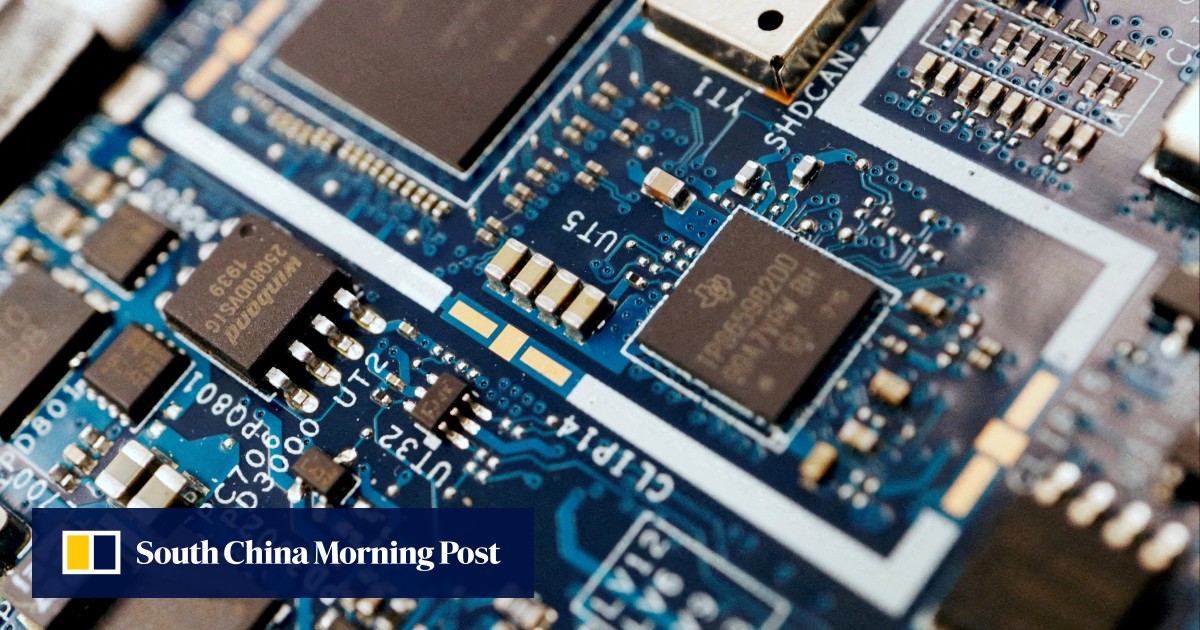
Semiconductor innovation is increasingly constrained not by ideas, but by the time, cost, and complexity of turning those ideas into production silicon.
As advanced chips become larger, more specialized, and more difficult to verify, engineering teams face mounting pressure to improve productivity without compromising quality or increasing risk.
Traditional design workflows, built around highly manual verification processes, are struggling to keep pace with the demands of modern AI, HPC, and cloud infrastructure development.
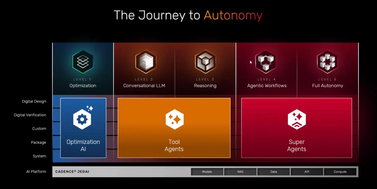
In this Cadence whitepaper, explore how agentic AI is reshaping semiconductor design by introducing autonomous agents capable of reasoning, planning, and executing complex verification tasks.
Read this Resource