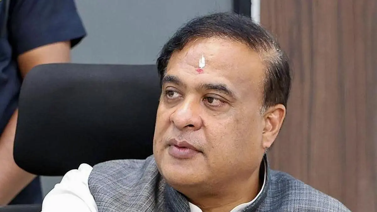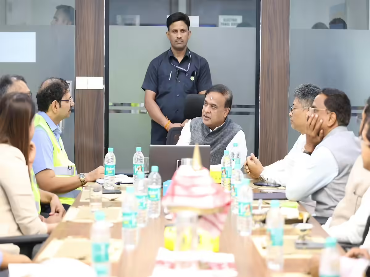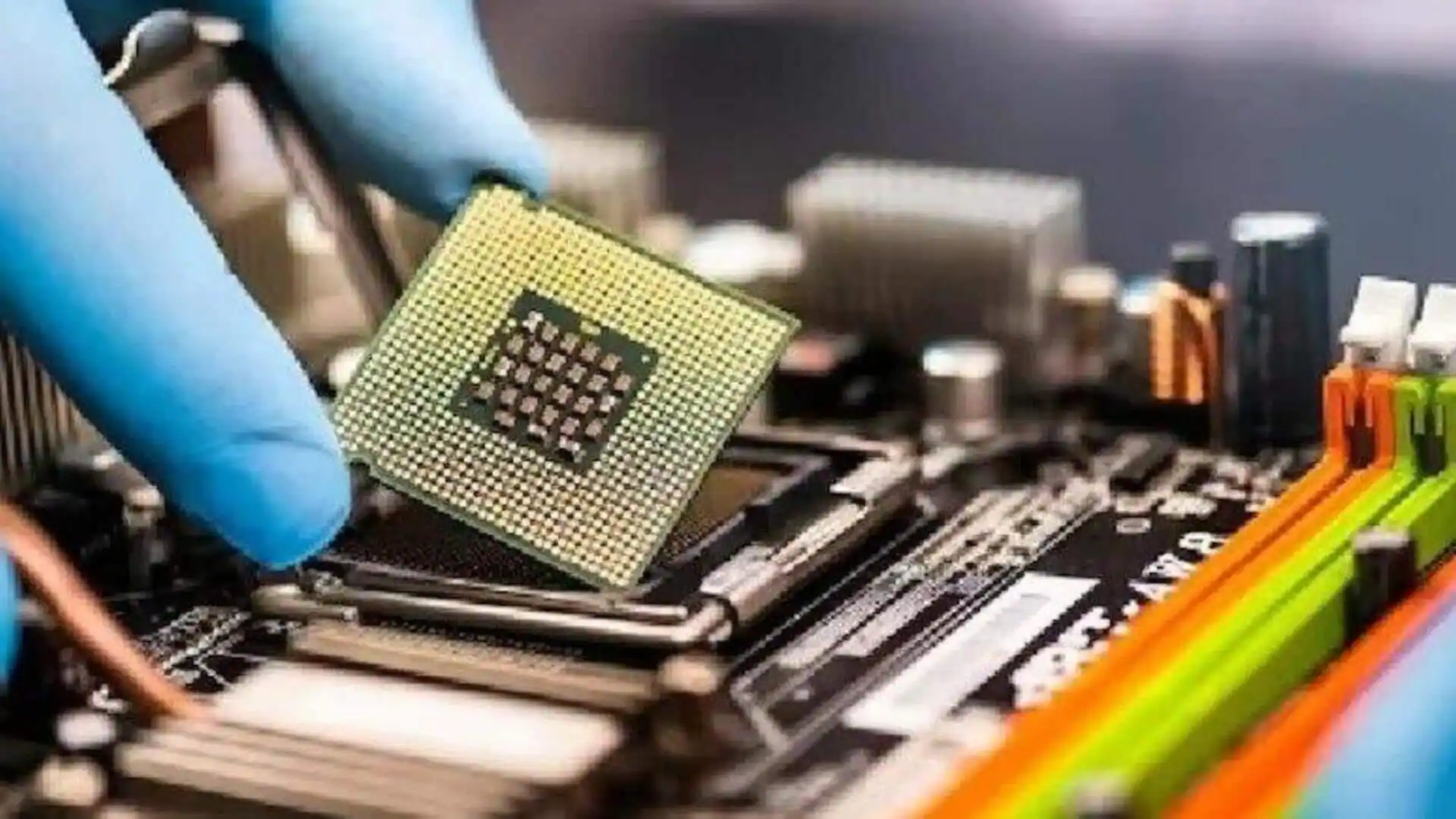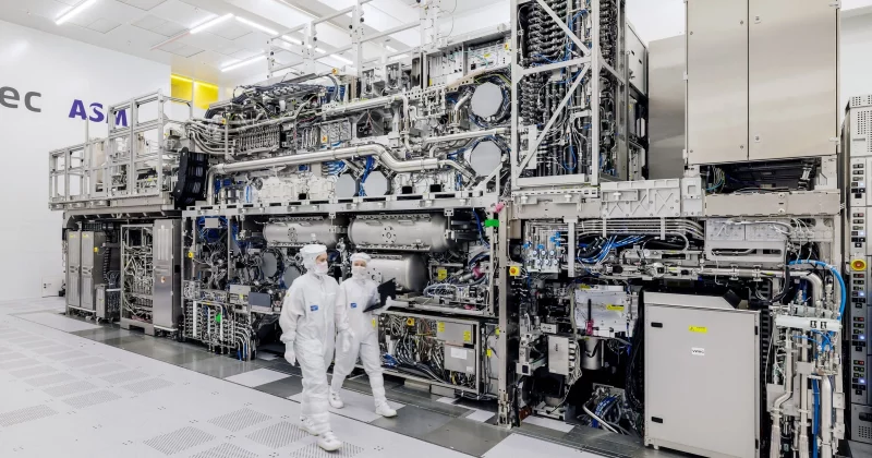
Tata Electronics plans to start chip packaging for global automotive and industrial clients at its upcoming outsourced semiconductor assembly and test (OSAT) facility in Assam, said people aware of the matter, providing a boost to the country’s semiconductor manufacturing ambitions.While the Tata Group company has already initiated small-scale shipments from its first commercial OSAT facility in Vemagal, Karnataka, the strategic pivot to the greenfield high-volume manufacturing unit in Jagiroad, Assam is aimed at building trust among global clients about the company’s capabilities while ensuring immediate scalability to meet surging automotive and industrial demand, the people said.“Tata Electronics has decided to ramp up operations by taking a small portion of the upcoming Assam facility for early qualification,” said one of the persons cited above. "This is being done to accelerate timelines and move in equipment as the facility comes up so that they are raring to go when full-fledged operations take off by the end of the year."Early qualification for cleanrooms — often referred to as the initial, preparatory, or pre-operational stages of validation —is a proactive approach to ensure the facility meets required standards before full, routine, and in-operation production begins. This approach reduces risks and prevents costly re-engineering later."They're (Tata Electronics) speeding up the work rather than waiting for the entire line to be ready or the entire building to be ready," the person said.The Rs 27,120 crore Jagiroad facility will feature one million square feet of cleanroom. The company is shifting a product line to Assam while continuing operations in Vemagal.A team from Vemagal will move by this month-end to handle the manufacturing transfer, replicating their activity in the upcoming unit in Jagiroad."Tata Electronics will continue with that (Vemagal) capability and run a small portion of the large facility in Assam that they will move into either this month or next month," a second person said. "This is the first step to ramping to a peak, and by September, the company will move many hundreds of tools, so that by the end of the year, the large facility is ready. It is debugging, learning, transferring, doing the logistics and getting the ecosystem ready."Tata Electronics didn’t respond to queries.Assam chief minister Himanta Biswa Sarma Wednesday visited Tata’s OSAT facility and said he was happy with the progress attained jointly by the project team and the state government."Production will start very soon from this facility, marking the official rollout of Made In Assam semiconductor chips," Sarma said in a LinkedIn post. "The Jagiroad semiconductor plant is a landmark project for Assam and for India’s semiconductor ambitions. The facility will have the capacity to produce up to 48 million semiconductor chips per day, catering to critical sectors such as automobiles, telecom, consumer electronics and AI driven devices."The phased launch would allow Tata Electronics to prove the unit’s operational readiness, and potentially capture market share ahead of schedule.Neil Shah, vice-president of research at Counterpoint Research, said it was the standard playbook for any capital intensive front-end or back-end fab rollout."Turning on the first cleanroom in a phased modular ramp way makes it operationally efficient, de-risking the learning curve," he said. "It allows the engineering teams to smooth out process yields, calibrate lithography/metrology tools, and perfect the logistics framework on a smaller footprint before turning the knob to full capacity."Shah termed it a “prudent strategy” that allows the company to match steps with demand trajectory.He explained that in the OSAT business, operational readiness is verified by metrics around process nodes such as 'yield rates' and 'utilisation rates.' Once that is proven, Shah said the company can take in more orders and keep the fab utilisation rates up to remain profitable.“This will enable the flywheel effect for Tata to scale,” he said. “Thus, close partnerships with leading supply chain players such as ASML and others from wafer to packaging are crucial to get up to the speed faster.”Tata Electronics on May 16 signed a memorandum of understanding with Dutch semiconductor equipment maker, ASML, for lithography tools, critical for India's first fab and advancing of the semiconductor manufacturing ecosystem in India. ET was the first to report on September 25 that talks were on between Tata Electronics and ASML for a partnership.
Tata Electronics plans to start chip packaging at upcoming Assam unit - The Economic Times
While the Tata Group company has already initiated small-scale shipments from its first commercial OSAT facility in Vemagal, Karnataka, the strategic pivot to the greenfield high-volume manufacturing unit in Jagiroad, Assam is aimed at building trust among global clients about the company’s capabilities while ensuring immediate scalability to meet surging automotive and industrial demand.
697 words~3 min read